Vibration and shock analysis of a PCB with Ansys Sherlock: predicting FPGA reliability and robustness
Written by Evan Smuts1, in collaboration with Shane Martin2
1 Application Engineer at Qfinsoft
2 Senior Mechanical Design Engineer at NewSpace Systems
Company Profile:
NewSpace Systems (NSS) is a trusted multinational spacecraft components and sub-systems manufacturer headquartered in South Africa, with branches in North America, Europe, and Oceania. Leaders in the area of Guidance, Navigation and Control (GNC) products, NSS are supporting the majority of the commercial spacecraft manufacturers, including several blue-chip companies and constellations of 500 satellites and more.
NSS is focused on delivering high-quality solutions and services. Whether offering clients access to flight proven off-the-shelf GNC products or, working closely with clients to develop custom solutions, the NSS team understands that each mission is unique and strives to enable the mission success of our partners through close collaboration. In space failure is not an option and therefore manufacturing is done by technicians who closely follow the rigorous ECSS standards and are certified by the European Space Agency (ESA). NSS state-of-the-art cleanroom facilities comply with the ISO 14644-1 standard, with their Quality Management System ISO 9001:2015 certified.

Intro:
FPGA (Field Programmable Gate Arrays) are integrated circuits that can be programmed or reprogrammed after manufacturing. They form the brain of any modern control circuitry. It is critical for mission performance that these components have 100% reliability, under all operating conditions. For NSS’s products, they also have to survive the rocket launch into space, which can be a challenge on its own due to the intense vibrations and shock loads that may occur with the rocket blasting away beneath it.
To prove reliability, the printed circuit board (PCB) with all it’s components (including the FPGA) must be tested against certain standards to demonstrate that it will survive the full range of environmental conditions it will face during rocket launch and operation on the satellite. After vibration testing, NSS noticed that some of the leads on the FPGA were cracked (figure 1 and 2). This would lead to component failure, not only of the FPGA, but also the system that it controls. While NSS had ideas on how to mitigate the lead failures, it can be very expensive to redesign the PCB and test it to failure, only to have to repeat the process to test another iteration. That is why they turned to simulation.
Working together with NSS, we used Ansys Sherlock to simulate the PCB under the different test conditions in order to identify the cause of the failures, and test different mitigation strategies. Once the Sherlock model was set up, testing new designs would take hours, instead of weeks.
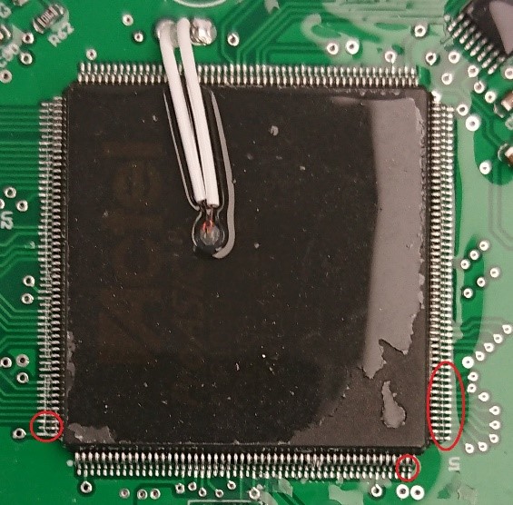
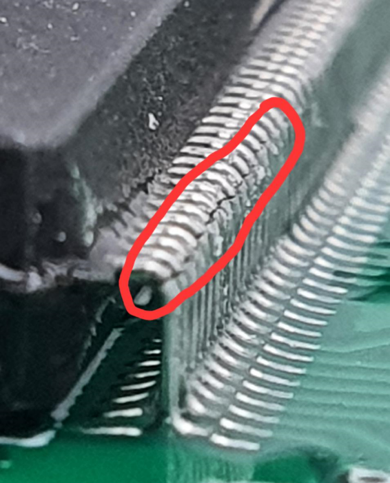
Figure 1 Figure 2
Importing and defining the model in Sherlock:
One of the great features of Sherlock, is its ability to directly import existing ECAD (Electronic CAD) files of the PCB. This means Sherlock is simulating exactly what the PCB designer has created, and it does not have to be redrawn. Sherlock then uses that ECAD import as the basis for both its internal simulations, as well as creating full, 3D, FEA-simulation-ready models to be used in an external FEA simulation tool. Typically, one would work with the common ODB++ file format, though some packages, like Altium, have an Ansys converter tool to produce the Ansys EDB file format. This puts the design into a format easily read by all Ansys electronics software.
Sherlock imports all the trace layers (with the trace patterns), as well as all the component information as defined in the ECAD modeller (figure 3). Component location is defined by the ECAD file and overlaid onto the layer plots (figure 3). It is possible to rotate or move components around, if necessary.
Another strength of Sherlock is its large library of component specifications, many supplied by the manufacturers themselves. Component package definition is picked up by the Sherlock Parts Library (figure 4a) and automatically assigned to each component. so detailed information on the package type, lead shape, construction material, thermal properties, etc. are linked to each component in the list. Non-standard parts can be manually assigned, or new ones created from the existing templates (figure 4b). The closer the definition is to the actual component, the more accurate the lifetime prediction will be. Admittedly, this set up can take a while the first time around, especially if you have lots of unique components on the PCB. But once the initial definition of the components is done, everything else goes pretty quickly, by simulation standards “A handy trick to speed things up” use an Approved Vendor List (AVL) to align your component part numbers with those in Sherlock. So even if your internal part numbers don’t exactly match the manufacturer’s ones, Sherlock can still link the information in the part library to the correct parts in your PCB import in only a few mouse clicks.
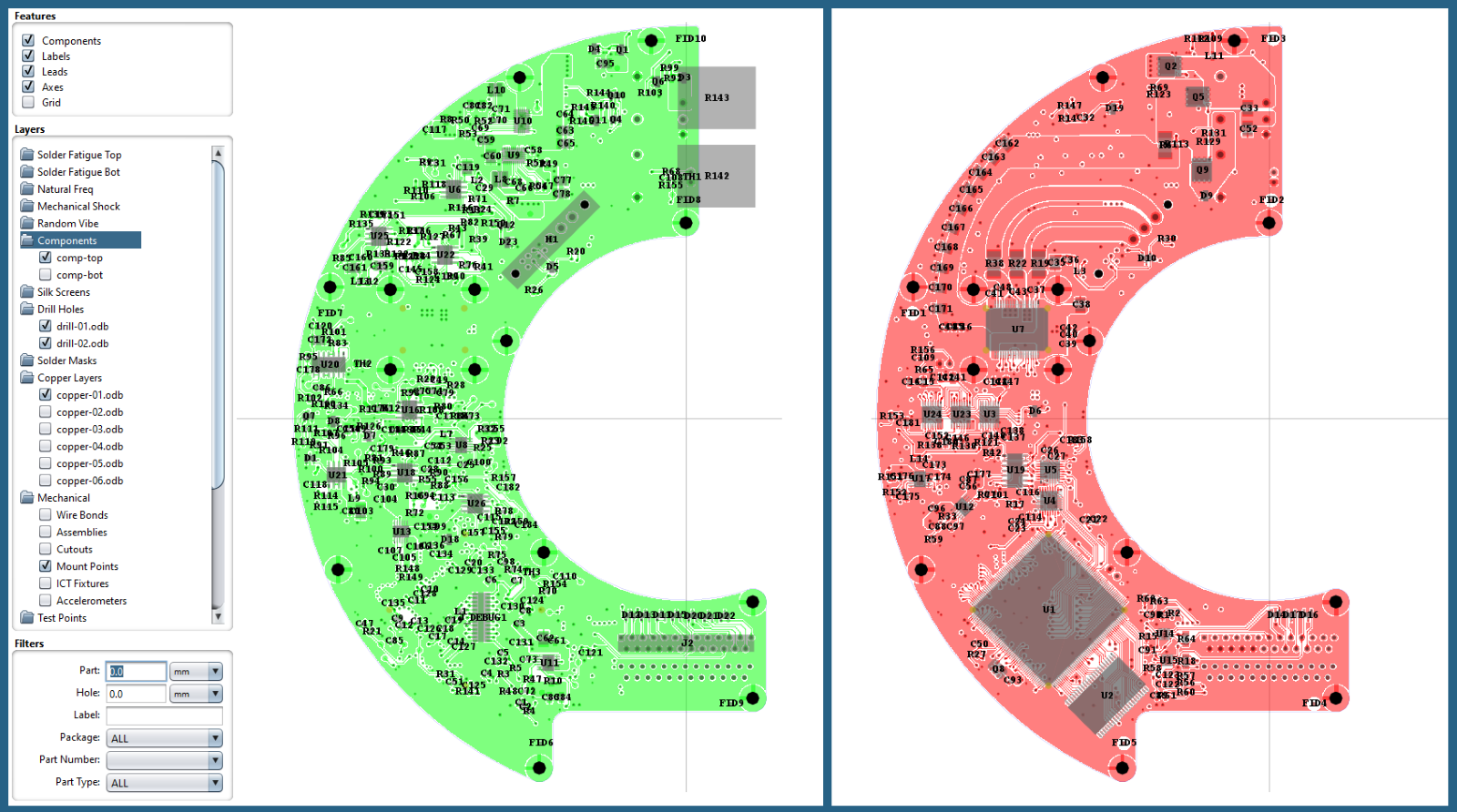
Figure 3
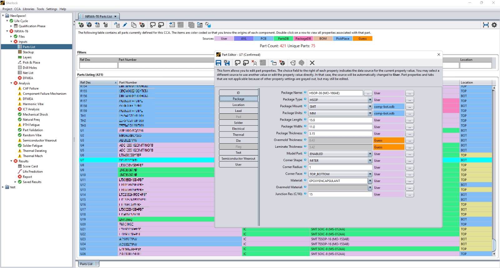
Figure 4a
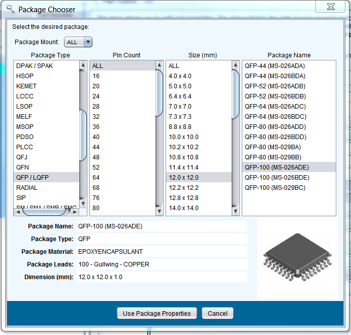
Figure 4b
All this setup work to create a fully-defined parts list pays off down the line. Apart from making significant changes very easily, Sherlock can actually be used as a pre-processor for 3D FEA models. Information from the trace layer thickness, and component dimensions is be used to generate a full 3D model of the PCB (figure 5). Even the leads can be modelled if required, they will be drawn based on their dimensions and type (e.g. gullwing, C-lead, leadless, etc.). Modelling of the leads was necessary for this project, as failure in the leads of some components was expected. Sherlock also quickly creates a 3D FEA mesh of the PCB and components, saving many hours in a meshing programme trying to properly capture all the small details. So even if your goal is not to use Sherlock for analysis, it can be a powerful first step in the workflow.
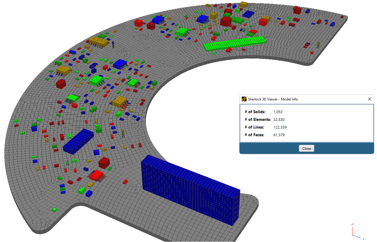
Figure 5
Some other useful PCB features that can be created “on the fly” in Sherlock are board mounting points, and potting/staking adhesive regions. These features are created on top of the existing PCB design, and so can be changed easily without affecting the underlying design layout. For example, mounting points usually have space left for them on the layout design where the holes are drilled through the board (large black circles in figure 6a). But the exact detail of how the PCB is mounted is lacking. In Sherlock, we can define the type of mounting that we plan to use in that location (figure 6b). The type of mount affects how the load (e.g. shock, or vibration) is transferred into the board material. Also, because the mount information is added in Sherlock, and not strictly tied to the ECAD design, we can change things around to test different scenarios, e.g. add extra mounts, or change their locations. All without changing the original ECAD design.
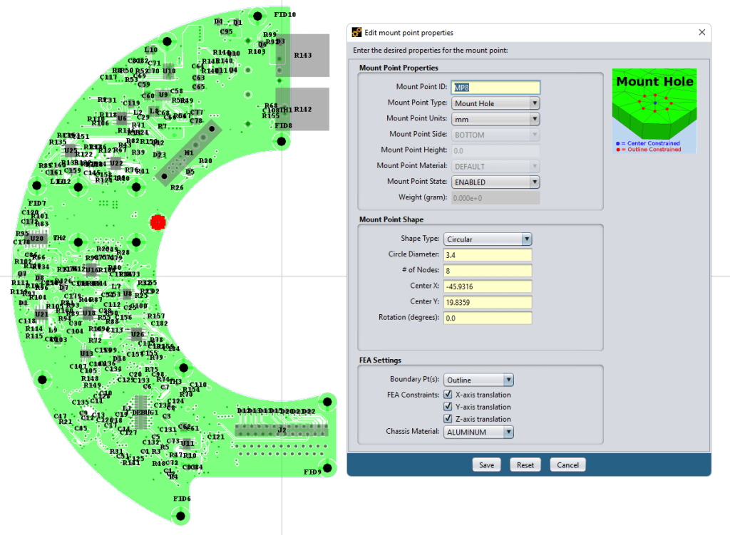
Figure 6a
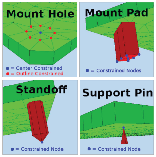
Figure 6b
Life Cycle Events:
The Life Cycle defines the desired reliability goals for the project. Life Cycle Events define environmental stresses that the PCB will experience over the project lifetime. These events can be once-off, or cyclical events that occur regularly over the lifespan of the product. Fatigue failure from cyclic loading is an important consideration when estimating the lifespan of a PCB. Sherlock can calculate both thermal and mechanical loading events. For these certification tests, three mechanical events were of interest: Random Vibration, Mechanical Shock, and Harmonic Vibration. Each event is defined with unique loading profile. For example, the random vibration loading event related to the rocket launch is shown in figure 7, with its associated vibration Power Spectral Density (PSD) statistical profile (figure 7b). Life cycle events can be considered individually, or the cumulative damage from successive events can be combined to predict the lifetime of the components.
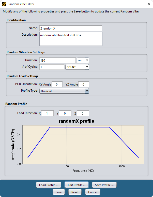
Figure 7a
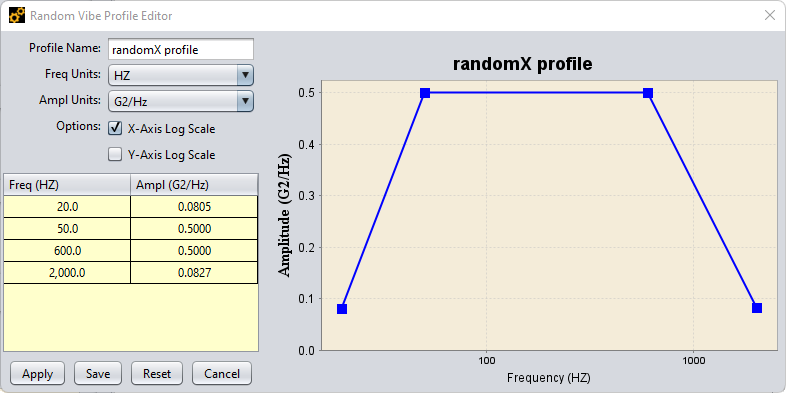
Figure 7b
FEA modelling – Original model:
While Sherlock can do some basic analysis itself (e.g. solder fatigue), full mechanical loading simulations do require an external FEA solver. In our case, Sherlock interfaces seamlessly with Ansys Mechanical, running this flagship FEA solver in the background. The results are then interpreted by Sherlock. To start, we run a modal analysis to identify the natural frequencies of the PCB, which is influenced by the board layers, and component location and lead types. Staking and mounting points will also affect the stiffness of the board.
For this project, we only had to consider frequencies between 20 and 2000Hz (required for the random vibration analysis). Sherlock identified five modes, ranging between 991 and 1829 Hz. This meant that we could not perform the Harmonic Vibration analysis, which required modes below 200Hz. Inadvertently, this result indicated the PCB would be fine during the Harmonic analysis.
For random vibration (RV), we considered vibration in all three axes (X, Y and Z). Displacement contour plots show how the RV displacement is dominated by the first natural frequency (compare the shapes in figure 8 – red indicating higher displacement). While the general performance of the board was good, Sherlock calculated outright failure of a component in the Z-axis vibration – the FPGA! Sherlock predicted it had a 100% chance of failure, with multiple leads exceeding the strain limit. We see an almost identical correlation between high lead strain and cracked leads identified in the experimental testing (inset photos in figure 9). It is very comforting when the simulation matches what you see in reality! Now we have great confidence that any further predictions will be faithful to the actual behaviour.


Figure 8


Figure 9a

Figure 9b
FEA modelling – Mitigation testing:
To try prevent lead failure of the FPGA, we looked at adding staking to the corners of the FPGA (figure 10a and b). This refers to using resin or adhesive material to either glue components together, or to the board. The staking adhesive would anchor the chip to the board surface, and take some of the load off the leads. This was evaluated during experimental testing. Fixing the chip to the board increases the stiffness of the board, which thereby increases the natural frequencies. After running the RV analysis again, we can already see an improvement in the performance. Sherlock’s lifetime prediction indicates that some leads unfortunately still do fail, but we have less failures than before and this will only occur after 2.3 years. This is significantly longer than the previous simulation. Which is great news, and shows we’re on the right path. Stress and the strain plots highlight the new load path through the staking points which reduces the load through the FPGA leads. However, staking only reduces strain in some areas of the FPGA are most likely because the board shows a similarly large deflection in that area to the previous case. So, there is room for improvement with this approach. A few more simulations would indicate how best to use staking to get 100% reliability.

Figure 10a


Figure 10b
Conclusions:
Through this short project, we were able to show how we can use Ansys Sherlock to efficiently model a PCB with all its components. After running some simple FEA simulations, Sherlock was able to replicate the exact location of failure we identified in the experimental testing. This gave us great confidence in the use of simulation to analyse the PCB’s mechanical performance. We were able to identify the chip staking and mounting points as areas where easy changes could be made to improve the PCB reliability. This will be verified during future experimental testing. The FEA-ready 3D model that Sherlock created will also be used in more detailed FEA studies, which will include the housing and real mounting points.

Related Posts